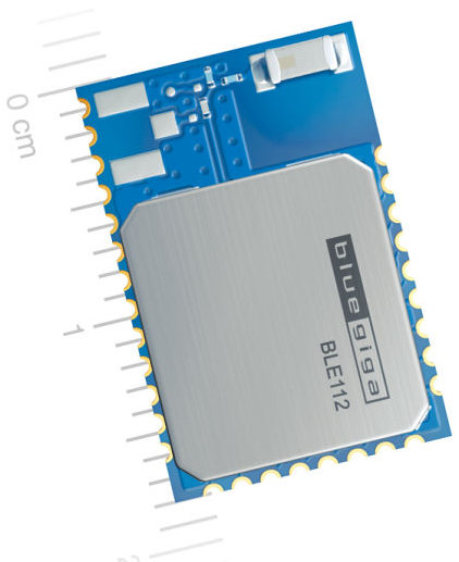
Bluegiga BLE112
To perform BLE-related development, I settled on the Bluegiga BLE112 for a number of reasons.
One was the BLE112D, a USB dongle version of the chip, which simplified development for the platform on both laptop and microcontroller (only one API to learn for both).
Another was the fact that it is powered, like many other BLE solutions, by a Texas Instruments CC2540 –a powerful little SoC for which I already had a CC debugger/programmer on hand (to perform firmware uploads).
Most importantly, for me, was BGLib–a sweet API distributed by Bluegiga to interact with the BLE functions–though with this module you could just as well use the on-board BGScript and avoid the external host all-together.
To get started, you need some way to connect the (surface mount) BLE112 to your host (e.g. Arduino). As I wanted a general purpose solution, that I could re-use in multiple projects, I developed the BLE112 USB breakout board presented here. There are other solutions available, but I went this way because I wanted:
- a homebrew solution I could easily make (on a single-sided printed circuit board);
- a general purpose board that would give me access to all the pins on the device;
- a board that included connections for the TI CC2540 programmer, as well as USB (“raw” and through a mini USB connector);
- something I could power from any supply (the BLE112 expects between 2V-3.6V, unlike most Arduinos which run at 5V); and
- a system that would have roughly the same layout as the BLE112 itself, such that the leap between prototyping with the independent board to having an on-board BLE would involve little change to the underlying circuit layout (one of the reasons it doesn’t have the same form factor as a standard Arduino shield, for instance).
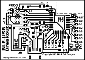
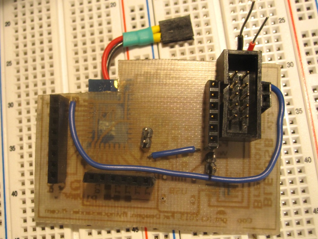
The result is the BLE USB Breakout Board:

BLE Breakout Board
With this board in hand, you’ll be able to interact with the BLE112 chip, and scan for/connect to slaves as master/client or advertise and act as slave/server. If you also use Eagle to design your circuits, you can download a parts library to use in the design of your own circuits, such that you can make custom boards that plug into the BLE breakout like this one:
example use with a mega328-based PCB
by adding the BLE breakout to your circuits from the library:

Eagle library BLE breakout part selection
In the following, we’ll go over everything you need to make your BLE112 breakout board.
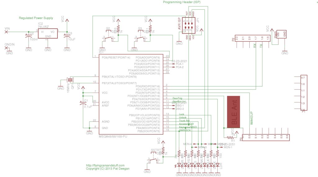
Circuit Theory of Operation

BLE112 Breakout Board Schematic
The circuit itself is very straightforward, as it doesn’t really do anything but provide power and access to all I/O pins:
Other than the pin headers, a few capacitors (to smooth the power source), a voltage regulator (to ensure the module is fed a safe voltage) and the BLE112 itself, the other components are pretty much optional.
I used the L78L33AC voltage regulator because it provides the 3.3V we need, comes in a relatively easy to deal with SO-8 package and I had some on hand. Another regulator, with a lower dropout voltage, might be better but this is what we gots at this stage.
One thing you may notice is that some connections may seem “upside down“. For instance, the CCPROG header. Because we want to keep everything on a single sided board to keep it easy to make this at home, all the SMT components go on the side of the copper trace but all the headers are inserted on the opposite side. This way, their leads are easy to solder on but it implies we need to do a little bit of customization on the pinouts of things like the CC programmer, so that the #1 pin–normally upper right–ends up being “lower right” when seen from the top.
Anyhow, all this is handled in the schematic and the PCB you will print out. You’ll just need to remember to put the headers on the other side!
Components
All the resistors, caps and LEDs used here are packaged in the (relatively) large 1206, to make them easy to hand solder. Core Components
| Core Components | ||
| Part | Value | Package |
| BLE112 | The BLE112! | |
| IC1 | L78L33AC | SO-8 |
| C1,C2,C3 | 1uF | 1206 |
| R1 | ~56R | 1206 |
| LED1 | SMT LED | 1206 |
You also need some male and female SIL 0.100″ pin headers, as well as a 2×5 male (ideally shrouded) header for the cc programmer.
If you intend to stick power directly into it (bypassing the voltage regulator, as I had to do when running on top of a 3.3V-powered microcontroller) and want to be really certain you don’t fry the BLE module, you can add a 3.3V zener diode, Z1 in a 1206 package (positioned on the pads just below the “t” of Breakout on the board). There’s a place for it shown in the placement diagram below.
USB Connector
If you want to use the USB connection, you’ll need a mini USB surface mount connector along with
| Part | Value | Package |
| R2 | 1.5k | 1206 |
| R3,R4 | 33R | 1206 |
| C4,C5 | 47pF | 1206 |
Note that I’ve actually fed the USB+ and USB- directly into the optional USB header without issue, but using including the parts above in the path is recommended.
PCB Construction
The BLE USB breakout board will look something like this when ready for soldering:
BLE Breakout board trace
NOTE: do not use the above to print your PCB, it’s scale is incorrect. Head to the Resource Download page to get valid resources.
In the following, the illustrations will show some variance as they were taken while building an earlier iteration of the breakout board. The changes are minor and won’t impact the instructions or your understanding.
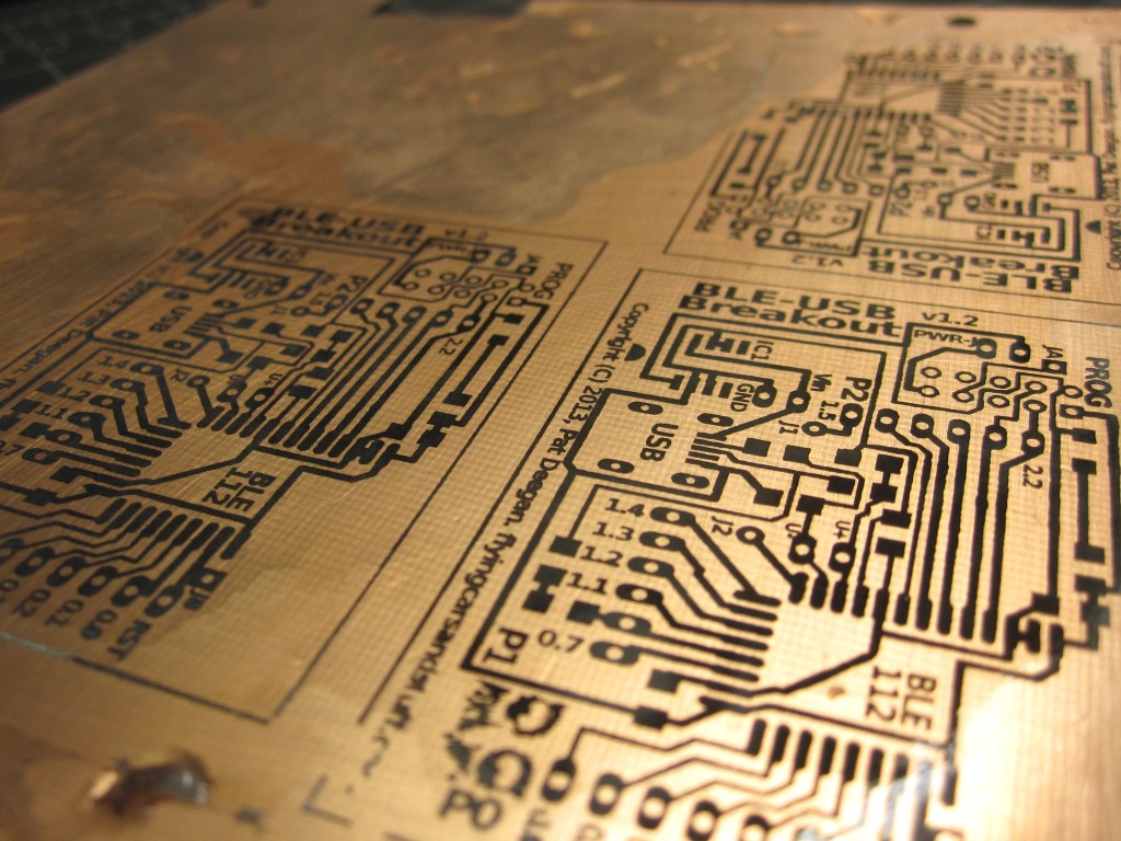
I started, as with all my kitchen-made prototypes, by printing the (inverted) PCB on magazine paper and transferring it over to copper (as described here).
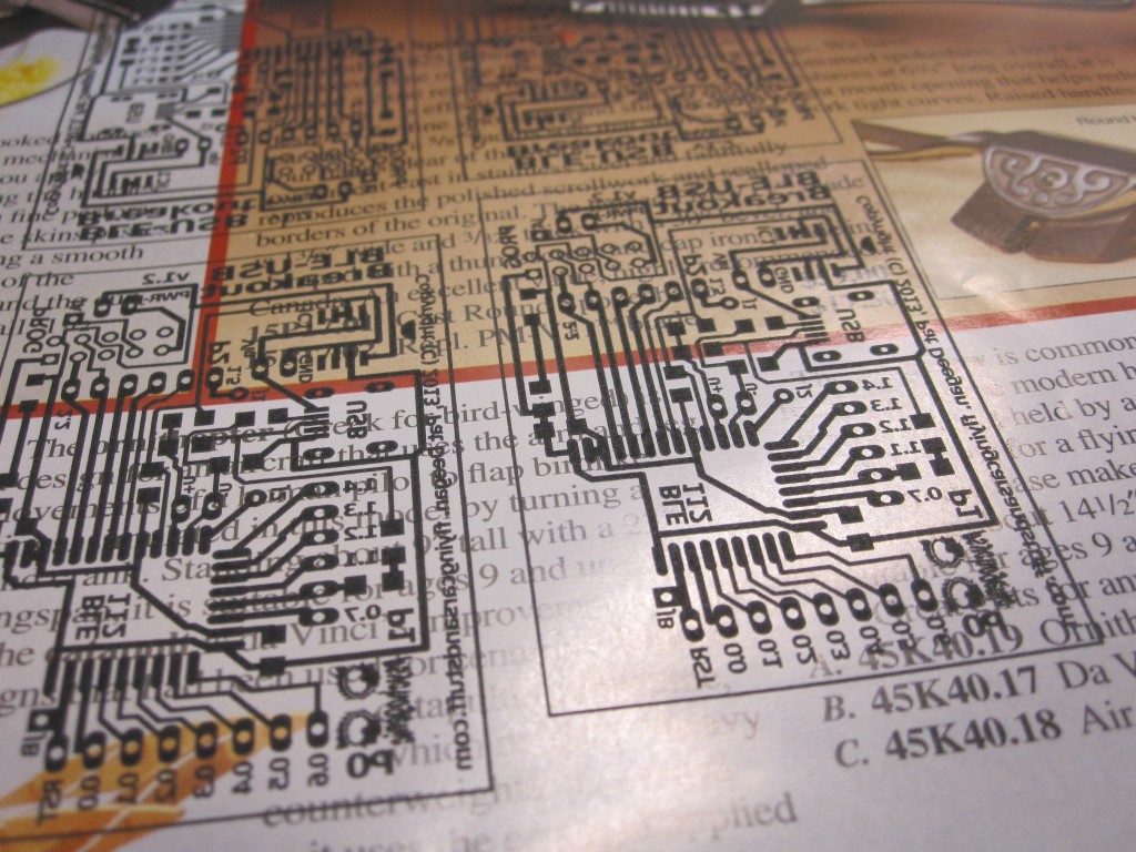
PCB printed on glossy paper
PCBs transferred
After etching and cleaning, the boards were ready for action.
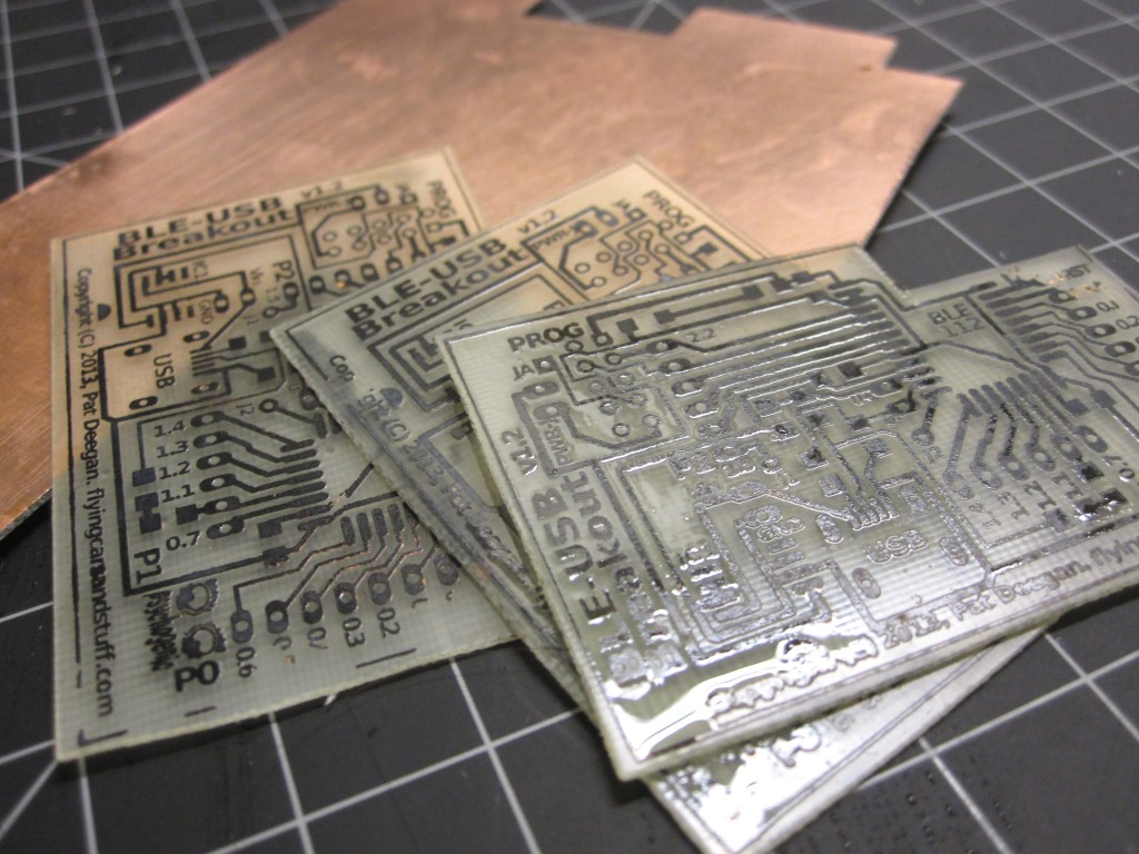
Etched PCBs
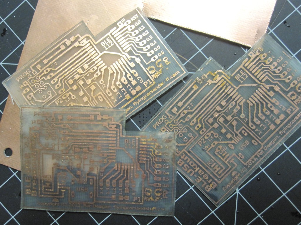
PCBs ready
There isn’t supposed to be anything, even dielectric, interfering with the BLE112 antenna. To minimize risk, I sliced out that part of the PCB, leaving a notch in the upper right corner.
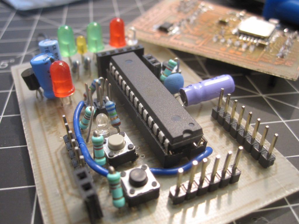
The components are placed as show in this diagram.

Component Placement
As mentioned, some are required but many are optional.
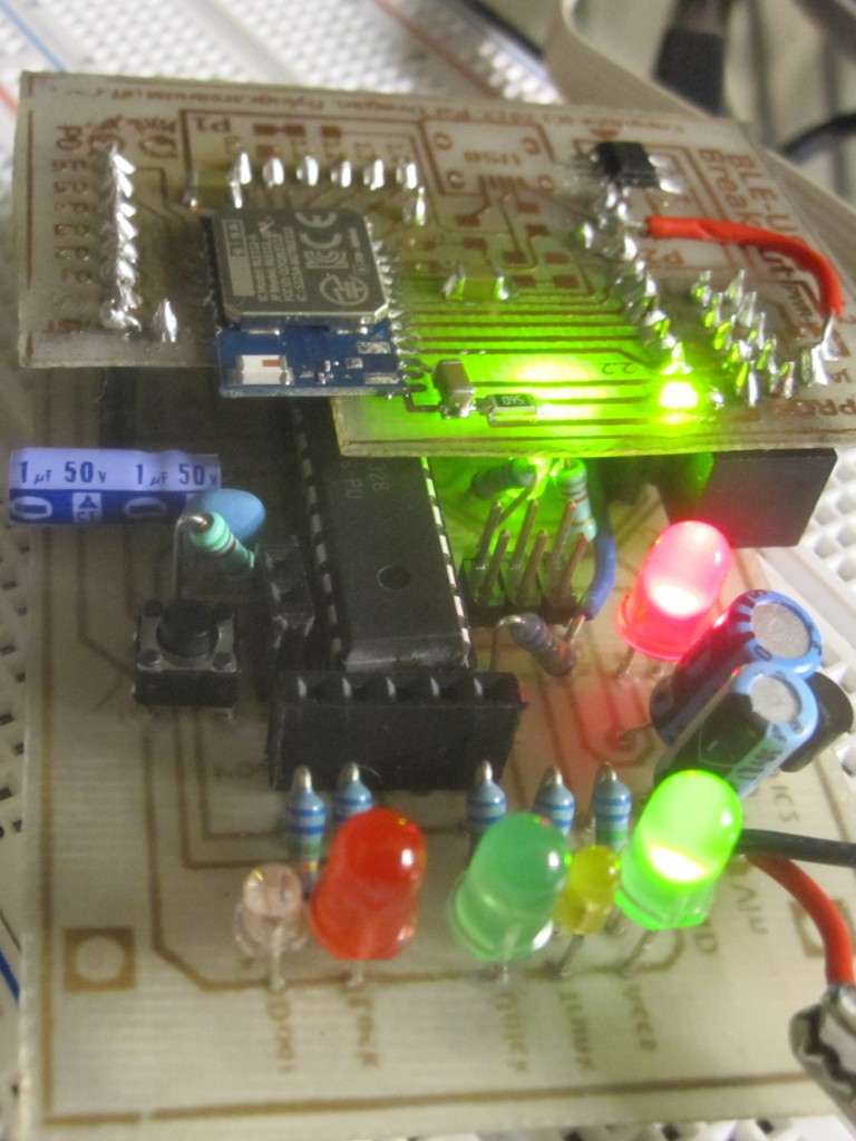
You can hand solder the parts pretty easily, but I have solder paste and a source of hot air and find the solution works pretty well. I have to admit I gooped on the solder paste pretty thick and carelessly, and wound up needing to do some cleaning and cooked my board a bit much. On this board, to get rid of solder bridges underneath the BLE112, I needed to heat the it so much in fact, that it actually de-soldered one of the parts. Ah well, messy but still functional.

PCB (slightly over-) pasted
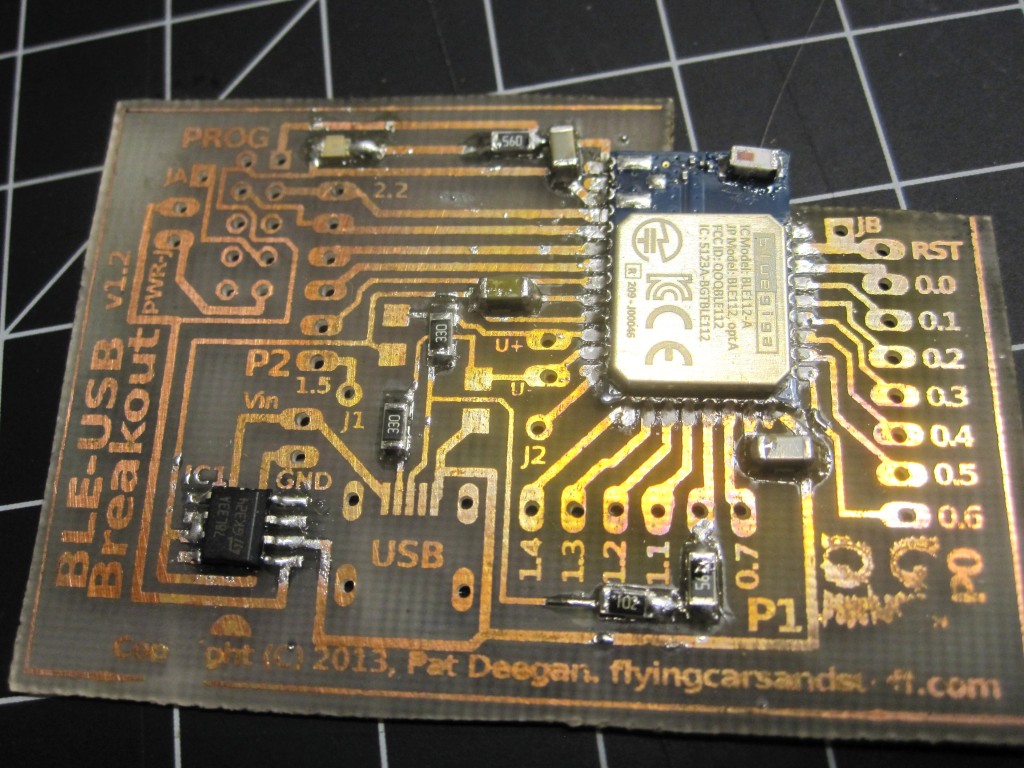
Messy but functional: board soldered
The headers and two jumpers are placed on the other side. If you’re using a shrouded header for the CC programmer, do note the placement of the notch (towards the BLE112). This forces the programmer to connect the right way, and is a good idea. I actually put it in the wrong way, first time round, and made another mess putting things right. ugh.
I like to use female headers for I/O (because it makes inserting leads from a breadboard easy) but to use male pins for power. The choice is yours. For the jumpers, JA ties to JB and J1 goes to J2.
Header placement
Once it’s all put together and tested, you can use the library to build custom circuit boards that mesh perfectly with the BLE breakout:
Breakout board library component used in circuit.
BLE Breakout connectors on PCB
example use with a mega328-based PCB
Using the USB BLE Breakout Board
The breakout board does it’s best to make all the BLE112’s pins easy to connect to without rearranging them, such that moving from the breakout to a single board, integrated, layout will be greatly simplified. The breakout board exposes:
- all the I/O pins (ports 0, 1 and 2)
- the USB+/USB- pins
- the RESET pin (no external pull-up or anything applied)
pretty much exactly as they are on the naked hardware–the major difference being that the breakout handles power management. This all means you can interact with the breakout board as if it was a single BLE112 integrated into your circuit. I/O ports P0, P1 and P2 provide general purpose input and output (configured as per Bluegiga directions and described elsewhere [HREF] in this series), while some of the pins also serve alternate functions.
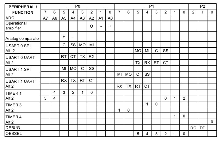
Alternate BLE112 pin functions
A few pins are brought out at multiple points, such as to provide a standard CC programmer or USB header.
Exactly how you use the hardware may depend on whether you are running code on-board the BLE112 (using BGScript) or simply using it as a comm-layer with another host (e.g. controlled through its USART by the external uC using BGLib). However, even when controlling the BLE11X from an external host, the I/O pins can be controlled and queried using BGLib and come in very useful when you run out of pins on your microcontroller.
From program-side details and examples, see the BLE client and BLE server tutorials.
BLE Project pages:
[siblings]