As a follow-up to my intro/tutorial, I’ll go over a few more lessons learned using Kicad including some tips that should be of help to anyone embarking on a similar journey.
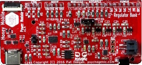
The power module project was selected for a first adventure using Kicad as it was relatively small while being non-trivial. The circuit holds around 100 components about half of which are unique, along with a number of non-standard chips (meaning I had to design library parts and footprints for them).
The Module
The power module designed has three main purposes:
- provide a bank of regulated supplies at specific voltages (3.3V, 3V… down to 1.8V);
- source power from various sources; and
- manage the rechargeable battery
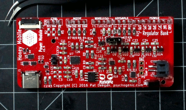
Power for the dependent modules can come in from a LiPo battery or wireless (Qi/WPC) charging, or USB. Since we wanted to support the newer USB Type C, a USB-C receptacle was used. However USB-C isn’t your grandpa’s USB and fully supporting is more involved than before.
As such, on top of actually protecting the lines from ESD, the power module hosts as USB-C controller to negotiate Power Delivery (PD), handle the reversible plug, switch the SuperSpeed lines as appropriate etc.
The wireless power involves it’s own power contract negotiation protocol–which all happens over the air through the air-gaped transformer created by the coupling of coils in the charger and the receiver side–and is managed through its own section near the center of the PCB.
Finally, the battery may be sourcing power or being recharged at any moment, so the board also includes a “gas gauge” to keep track of battery voltage, current consumption and temperature.
You can actually see the board and watch it in action in this short presentation:
Design Lessons
In addition to tips from the previous Kicad post, here are a few things I learned while working on the project.
Because this prototype was to be built in-house, most of the passives used were 0805 SMT components. Because of the uncertainty in using Kicad to produce the boards, for all of these the appropriate “hand soldering” footprint were selected (e.g. Capacitors_SMD:C_0805_HandSoldering for caps).

Turns out that this was overkill: the resistors and capacitors wind up taking as much space as many of the chips used and it all adds up to the board being a good deal larger than it needed to be.
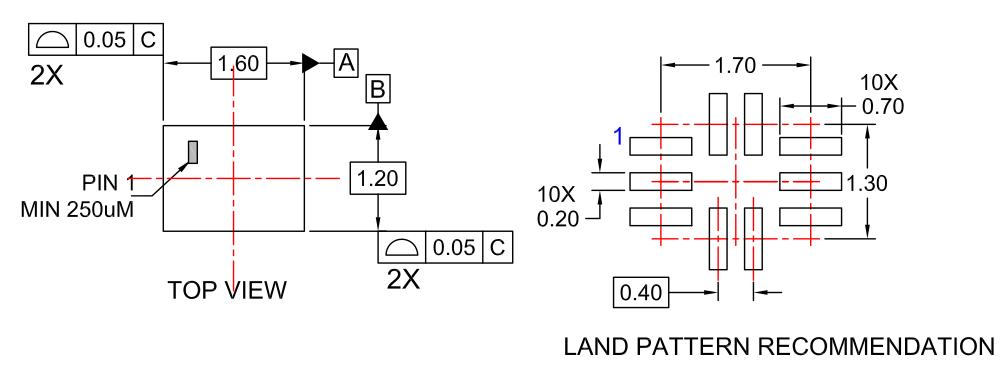
Admittedly, the above is a worst-case since the FUSB301 (a USB Type-C controller) is a small part with 0.2mm pads.
Still, regular footprints are now used in most cases for these components.
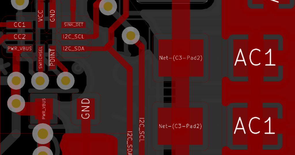
The other important lesson concerns one of the major gripes I have with Kicad in its current state: cut-outs.
The USB-C receptacle land pattern specified an annoyingly complex cutout for its back legs. This led to two problems with Kicad:
- having the cutout milled by the fab; and
- dealing with zone fills.
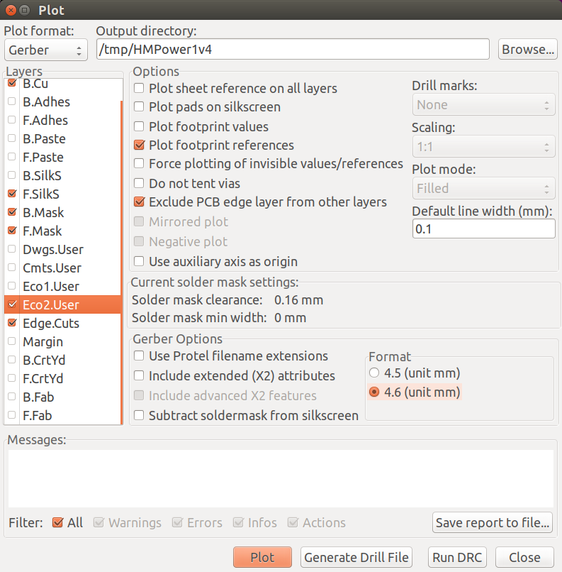
Since Kicad won’t let you specify that a segment is on the Edge.Cuts layer in the footprint editor, I’ve settled on reserving “Eco2.User” for anything involving part-specific milling.
Here’s a cut-out shown with and without the Eco2.User layer being rendered:
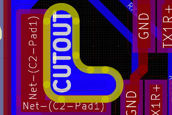
If you’re going to have boards like this produced, you’ll have to ensure that you actually keep all your cut-outs on the same layer (say Eco2.User) and not use that layer for anything else. You’ll also have to export it and get the fab to actually do the milling as specified.
Also, if you want to avoid having any fills actually intersecting the cutout, you need to remember to do a little extra work. Here, we couldn’t have the ground plane on the bottom shorting directly onto the USB-C shield, so a separate zone (connected to <no net>) must be created within the cutout with sufficient clearances and an appropriate priority level to keep any other fills from creeping in there.

Finally, though this caveat didn’t bite me until a subsequent project it is worth noting: when you are reworking copper traces on a board with fills, you must refill all zones (normally the “B” hotkey) to ensure there aren’t any new shorts between traces and zone fills, prior to exporting gerbers.
And that’s it for this project. Since then, I’ve done a number of boards with Kicad and have started becoming quite adept at using this excellent software. I wish you luck on your own projects!