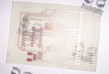
This document–a re-print of an old but still relevant and useful article I wrote–details the creation of professional quality printed circuit boards (PCBs) using a laser printer and easily obtainable tools and materials.
TOC
- Requirements
- Overview
- Laser Printers
- Which Printer?
- Printing PCBs
- Transferring The Image
- Etching The Board
- Finishing the PCB
Creating Printed Circuit Boards (PCBs) is easy and fun for the whole family! But read the disclaimer cheap NBA jerseys — heat and corrosive chemicals are dangerous ;-)
After you’ve prototyped and tested your circuit design, creating a PCB will provide a sturdy and reliable backbone for your circuit and will give your project a professional finished quality.
Using PCBs can even help reduce the time you spend building circuits, especially if you are producing multiple units, as you only need to follow a parts placement diagram (there’s no longer any need to worry about specific interconnections).
As is usually the case, there is more than one way to do it: there are
numerous ways to create PCBs. They range from the time-consuming and difficult to the fully automated and expensive. Here we will attempt to describe a method we’ve found ideal for small production runs (say, a few prototypes to a couple of dozen–when you reach the hundreds, it will probably be easier, quicker and cheaper to outsource) of single- or double-sided boards.
Requirements
To proceed with this technique, you will need access to a few tools and materials. These include:
- Laser printer
- Suitable glossy paper
- Copper PCB boards
- An iron
- Etchant
- Protective clothing, plastic tupperware, other stuff
Overview
Here is the technique’s executive summary. Print up the PCB traces on suitable paper and transfer the toner to the copper. Etch the board, Why remove the toner and drill. The PCB is ready.
Read on for a more detailed description of the process.
Laser Printers
A neat thing about laser printers is that the toner is transfered from the cartridge to the paper in a powdery form (unlike with inkjet printers, that use liquid ink).
In order to get the shapes and letters to stay in place on the paper, this
powder–which contains plastic–is heated, so that it melts and fuses in place.
When creating a PCB using a chemical etchant, you want to protect certain areas of copper from the chemical reaction (to form the pads and signal lines) and let the ferric chloride remove all the metal that remains exposed. There are a number of ways to do this: a sharpie marker will do the trick and so will laser printer toner.
So all you need is a way to get the toner from the printer to the copper. Sadly, PCBs are
usually too rigid to go through the printer so we must find another way. A simple solution is to print a mirror image of our PCB traces on a material to which the toner will bind only mildly, then heat the material to remelt the toner and get it to stick to the board. This is similar to the iron-on t-shirt technique.
Which Printer?
We’ve used a few different printers to perform this type of work: a few from the printer shop and our own Samsung.
I am uncertain of the make and model of printer from our habitual printer shop. The most difficult part of the process over there is explaining to the guy at the counter that he shouldn’t put his fingers all over our special paper and toner.
That and the cost of printing from CDs convinced us to purchase a laser printer.
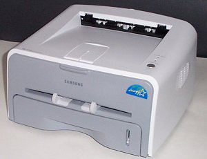 This is the printer we
selected: the Samsung ML-1710 laser printer. A number of reasons motivated our selection. The
printer offers very decent quality with a small footprint and great price (we even got an extra
$50 mail-in rebate from Staples).
Another very important factor was underscored by the printer test page (output by holding the Cancel buttons for 2 seconds). As you can see from the close-up, this Samsung printer is proud of its Linux support and even lists a number of distros. Performing a search on the Samsung Site for 1710 reveals a list of driver and
helper programs for all platforms, including Linux.
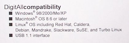
We didn’t even bother installing the drivers: the RH9 box on which we hooked up the USB printer allowed us to easily add the Samsung (using the redhat-config-printer utility) as an ML-1220 (suggested by many on usenet). Doing so allowed us to immediately begin using the printer–we even shared it through Samba, so the poor MSWindows users on the design side of the office could access all the laser goodness.
In terms of performance for our particular use, the printer works wonders. It outputs at a maximum of 600dpi, but we’ll usually prepare the PCB images at 400dpi so there’s no problem there.
Printing is fast and smooth and the resulting images are completely free of imperfections and artefacts. We might have access to a few more printer configuration options if we actually installed the Samsung drivers but the current levels meet all our requirements so there’s a certain lack of motivation.
Printing PCBs
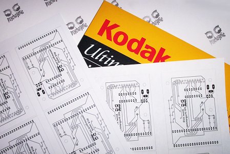 Second only to the type of
printer toner, the choice of paper is a very important consideration. You need to use a medium that will go through your printer and will preserve the printed image but won’t absorb the toner or bind it too tightly. For this, glossy paper is the Press answer. In this demonstration, we’ve used Kodak Ultima Picture Paper–specifically their “High Gloss” 71 lb (270g/m2)–as it works
well and should be available throughout North America and possibly Europe. It is their picture paper with the heaviest weight and is said to be useful for “Professional quality photographs”.
This also means that it’s expensive: $1 or more per sheet in small quantites. A fact discovered later is that you really can use many different types of glossy paper, including pages from the Times or any other magazine, and it works even better than “picture paper”.
To save time, effort and expenses it’s a good idea to combine multiple images to
try and fill the entire 8.5×11 page with PCBs.
Remember that these must be printed as mirror images of the final PCB
in order to be correct after transferring them to the copper board. On the left you can see an ordinary sheet of paper used during the trial run and (to its left) the glossy kodak paper with the 9 PCBs.
Transferring The Image
To proceed you will need a cut-out of a single PCB image from the glossy paper, a very
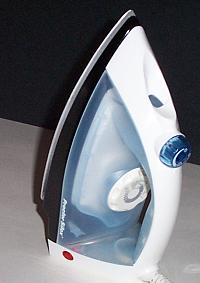
clean copper board and a clothes iron. The iron depicted below, a regular proctor silex model, had instructions stating that it should only be put to its intended use. Since we Metal purchased it with the intent to use it to create PCBs, I guess that’s ok ;-)
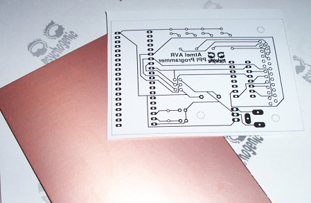
The PCB-to-be needs to be very clean. You can start by washing with hotwater and dish soap. Using acetone or alcohol to rub it clean seems to work well but may not be necessary. Make sure the copper is dry and that no soap or chemical residue remains.
Do not touch the copper with your fingers as you’ll spread greasy human juice which may keep the toner from sticking. You can gently sand the board, using very fine sandpaper.
Some have reported that using steel wool is a bad idea, is minuscule particles of iron get lodged in the board and eventually rust. When the copper looks clean, shiny and new, you are ready to proceed.
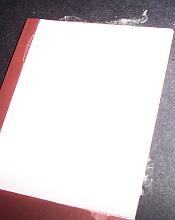
Place the PCB mirror image face down on the copper, ensuring it is correctly positioned. You can use a few pieces of tape to secure the glossy paper to the board but I find that, if you are careful when you begin to iron, the paper sticks and stays in place on its BALL own.
Preheat your trusty clothes iron, using the hottest setting its got (cotton, linen or above). Note that you may not want to use the iron on clothing after this procedure, because of potential residue or damage, so be sure to get the owner’s permission or purchase one specifically for the task.
Delicately place the hot iron on top of the paper and copper board. Our standard, ISO certification pending, technique is to leave the iron on the board for a few seconds before beginning to apply pressure.
Initial ironing motion is from the centre outward towards the sides. If
you are using the Kodak picture paper, you’ll notice that the sticky stuff on the back of the paper melts and spreads off the paper to the adjacent portions of the copper board (note the semi-transparent weirdness surrounding the paper–that is melted kodak
goop). This actually helps to keep the paper in place.
Iron the entire area of paper, pressing firmly and staying long enough to ensure the toner melts a bit and binds to the copper. How much is long enough? It’s hard to tell and you will need to experiment with your combination of iron and toner. For us, about 10-15 seconds per “spot” is good and a PCB of this size will take around 1 minute to 90 seconds.
When you are done, be careful as the board will be hot. Immerse the board setup! and paper in hot water for a few minutes (up to 10 if you’ve got the patience). This will soften things up a bit. If you are using the kodak paper, that melted-then-solidified goop from the back of the paper will turn into a slimy/sticky substance; you can gently scratch it off to aid in removing the paper.
Carefully remove the paper. If certain areas seem particularly difficult to peel off, you can try soaking a bit more. If everything went well, you will Bruksp?jkera have a copper board with your PCB pads and signal lines traced out in black toner, something like this:
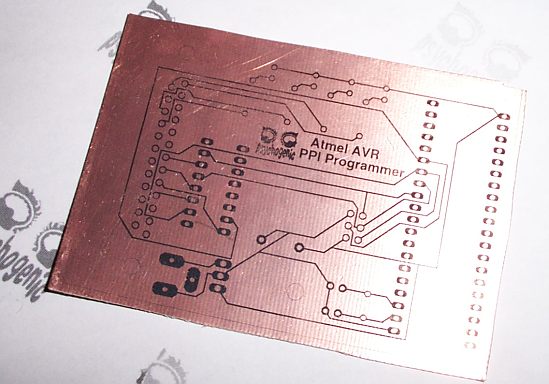
You can see that even fine lines, such as the contour, have been successfully transfered. The camera flash accentuates numerous small flaws and scratches in the copper but you can see these are mainly in areas which are to be etched away (uncovered by toner).
Etching The Board
The next step consists in removing unwanted copper from the board. You’ll need a couple of items to get this done. Before we begin: yes, you’ve read and understood the site disclaimer but this is the most dangerous part of this page:
you can get chemical burns, go blind and other nasty stuff so take a deep breath and think before you move. I don’t know what you should do if you get some in your mouth, eyes or ears so don’t do it.
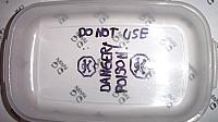 Item 1: a bin to perform the etching in. This container must be wide enough to accomodate your boards.
It must be made entirely of plastic or glass.
Tupperware works nicely but remember that some strange folks actually use these things to store stuff like food, of all things.
To avoid any possible future mix-ups, mark the container with a large, clear warning. Our resident tupperware artist (yours truly), having spent too many years using keyboards and Palm Pilot Graffiti, added his signature style to the recipient on the
left. In my defense, it is worth noting that in order to ensure the message would last I actually wrote it as a mirror image, on the outside of the container.
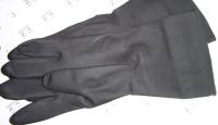
Item 2:
Protection. Protective clothing is a must. This includes industrial strength rubber gloves and eye-wear. A source of running water is also handy, as are paper towels and other means of repairing the unavoidable accidents–don’t wait until it happens and you’re wearing etchant-covered gloves to figure out how to clean up a spill.
 Item 3:
Etchant. You can use the classic, ferric chloride, as we do or go for Ammonium Persulfate crystals or other chemical solutions. All of them are nasty, so read
the bottle.
You won’t need a ton of etchant for a regular sized PCB. Start with a bit, enough to cover the board.
You can always add more if the reaction stops.
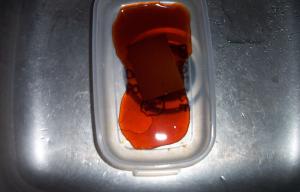
Just how much etchant you need and how long the process takes will depend on many things: the size of the PCB, the amount of copper on the board (both in terms of area and thickness). Somewhat hotter etchant will react faster than a cold solution but we like the ease and control that using room temperature etchant affords us.
Constant motion isn’t required but also helps reduce the etch time: some people use mechanical means, such as aquarium “bubble machines”, to mix it automatically.
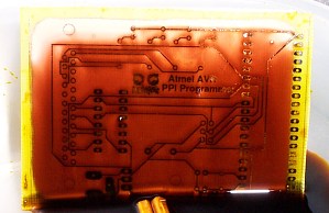
Regularly stir the solution, every couple of minutes, to ensure the board is in contact with fresh etchant. After a while, you will be able to see that the reaction has begun. The etchant solution will get filled with dark colored particles and the copper will begin to disappear. Removing the PCB from the solution for a few seconds will reveal freshly etched spots. Notice how the etchant quickly runs off the portions of the board which are copper free and how the process has a tendency to begin on the outside of the board:
After something like 50-75% of the copper has been removed, gently stir the solution (never use metal) on sway the container and keep an eye on the state of your board.
The process seems to accelerate in the final stages; this is only an impression but it can surprise you and lead to over-etching. Leaving the board in the solution too long will cause the etchant to eat at your signal traces from below, potentially causing breaks in your wholesale MLB jerseys traces.
When all the superfluous copper has been etched away, remove the board and rinse it with lots of cold water. You do not want to get a lot of etchant in your drain. Besides being really bad for the environment and probably being against the law, it may eat away at your plumbing. You should instead store used solution in an air tight, glass container (e.g. “Mason jar”) and store it, clearly labelled, along side your etchant. When the container is full of used etchant, bring it over to your recycling centre/dangerous waste disposal facility.
After the board has been thoroughly rinsed, you will have a PCB covered with toner:
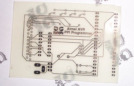
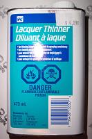
The fastest, easiest way to get rid of the toner is with lacquer thinner. If you buy this
exclusively for creating PCBs, 100 milliliters should last you two years! Lacquer thinner is extremely volatile, it catches fire easily and stinks–use wholesale NBA jerseys it outside or in a very
well ventilated area. All you need is to do is to get a small quantity on a paper towel and
quickly wipe your PCB clean. The laser printer toner will smudge and just about vanish.
Once that is done, you’ll be in possession of a PCB that looks like this:
Finishing the PCB
You now have a beautiful printed circuit board! Your work is not quite done, but ours is :)
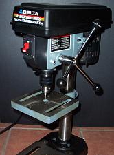 All that is left for you is to drill holes as appropriate, place your components and solder.
If you are using lots of ICs, a drill press or Dremel tool with the drill press attachment will be a great help.
We hope you found this HOWTO informative, useful and maybe even
entertaining. If you have any questions, remember that the universe is
just begging to answer all of them–experiment a little
and see. If you would like to share your experiences, hints and tips,
then don’t hesitate to
drop us a line.
