This small project provides high voltage, high-side switching for up to 8 independent loads.
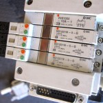
I had a project that used a set of four base-mounted pneumatic valves to control a set of actuators. The valves were “double-solenoid” setup such that air could be shunted to either “A” or “B” tubes for each of the four valves by switching 24 Volts on one of the two solenoid inputs.
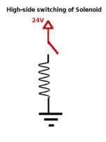
Since the set of valves used a common ground, this meant using high-side switching–i.e. the switching action happens “above” the load, between the 24V supply and the solenoid. For this to work, you need to use a PNP transistor or P-Channel MOSFET. In addition, I wanted to use a microcontroller (an Arduino, powered by 5 Volts) to control the valves and you can’t use a simple PNP switch circuit with a higher load voltage than the mcu‘s supply (first off the switch would always be closed and, more importantly, you’d probably burn out the microcontroller by feeding the pin excessive V).
The solution I came up with is presented here, with the schematics and layouts released under the Creative Commons Attribution-NonCommercial 3.0 (CC BY-NC 3.0) license.
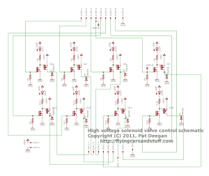
This board can be used to (high-side) switch 8 distinct valves, relays, or whatever using pretty much any supply voltage between 5V and 60V to drive up to about 9 Amps through the load. Values given here are for the 24V supply I was using, you’ll have to adjust the values used for the LED indicator resistors (the even numbered resistors, R2, R4… R16 in the schematic) if you are using different voltages.
Theory of operation
The circuit is basically a simple two-transistor switch, repeated 8 times. Each output pin, from the microcontroller, controls one of the odd-numbered (N-Channel 30N06) MOSFETs.
When the pin goes high, the corresponding MOSFET’s base is driven such that the switch is closed (current flows). This effectively ties it’s collector to ground, bringing it low and taking the base of the second (P-Channel MOSFET, an 11P06) to ground, closing that switch and connecting the corresponding solenoid control pin to the high voltage supply.
Since the P-Channel MOSFET base point (for instance the connection between Q1, Q2 and R2 in the schematic above) will be low when the microcontroller’s pin goes high, current will flow from the 24V supply through the LED and resistor giving a visual indication that the switch is active.
The odd-numbered resistors (R1, R3…R15) ensure that the N-Channel MOSFET bases stay low even if there are glitches during power-up, while the diodes (D1 through D8) are used to snub the current generated whenever the solenoid (inductor) is switched off and its magnetic field collapses. You can leave these out if your loads aren’t inductive, but including them makes the board useful under any scenario.
Notes
If you are using a different supply voltage, or plan to use the circuit in a number of different scenarios, calculate the LED resistor value by taking the specific LED’s forward voltage (e.g. 2V for a red LED), the maximum current you want to let pass through it (say, 15 mA) and the highest voltage source you’ll be using (e.g. 50V). Then, R = (Vsupply – Vled)/I so using our example numbers, the ideal value for the Rs would be:
(50 - 2) / 0.015 = 3200 ohms
So you could use the 3.3k but I’d probably overdrive it a tiny bit (16mA instead of 15) by using the 3k resistor, in cases where I’m using lower supplies as well (accounting for the higher voltages reduces brightness when using a lower supply, e.g. only 7mA gets through with a 24V supply using a 3k resistance).
Parts
| R1, R3… R15 | Odd numbered resistors, used to keep N-Channel bases low, anything around 10k should work |
| R2, R4… R16 | Even numbered resistors, used to limit current through LEDs. See Note above. |
| LED1-LED8 | Any LED you like, just make sure you calculate the associated resistor (even numbered, R2-R16) as described above |
| Q1, Q3… Q15 | Odd numbered Qs, N-Channel power MOSFETs, like 30N06L |
| Q2, Q4… Q16 | Even numbered Qs, P-Chanel power MOSFETs, like 11P06 |
| D1-D8 | Use a 1N4002 if you are going to switch a 50V supply (or more), otherwise you can probably stick with good old 1N4001 |
| Connectors | I like to use molex connectors, 9 pin SIL for I/O and a 2 pin SIL for the high-voltage supply. |
Creating the PCB
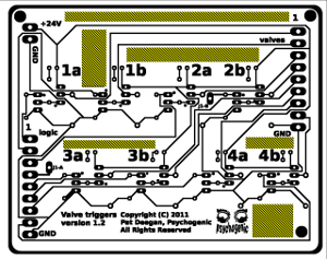
I created the printed circuit board using the laser printer toner transfer technique. You can save the (mirrored) layout, and print/transfer it as described in the DIY PCB HOWTO.
Don’t save this preview image, click on it and save the linked mirror version:
Layout
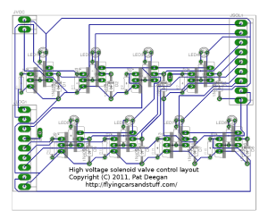
The board is quite symmetric and once you figure out the placement for the components on one of the switches, the others are all the same.
As seen from the below (the side you solder on, with the copper traces), the MOSFET pairs are back-to-back with the N-Channel on the left. The LEDs all have their cathodes (flat side, short lead) to the left. The 1N400X diodes all have their cathode (black bar) facing up towards the MOSFETs. The resistors can of course be placed however you like, just put the odd-numbered set to the left of the MOSFET pairs and the even numbered set between the pairs.
In order to get the traces routed on a single-sided board, for easy production at home, I had to use a single jumper. Solder a wire between the J1-A pad (connected to the fourth pin of the logic/input connector) to the J1-B pad (located near the centre, below the “2a” indication on the PCB).
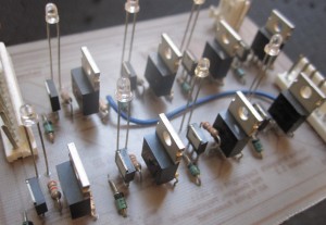
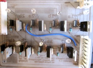
From the top, the completed board with the jumper looks like this:
I left the LED leads very long so they could pop through the top of the enclosure. Setup Molex or other connectors for the I/O and power supply. The lowest pin of each of the 9-pin connectors is ground, and each of the other 8 inputs controls the corresponding output pin.
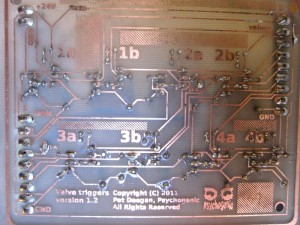
When done, you should have a PCB like so:
As you may have noticed, there were a few glitches in the toner transfer up at the top right. I completed the traces using solder and, in one instance, had to add a second jumper to get around the defect. Otherwise, the board came out pretty well.
Connect the higher voltage power supply to the two-pin connector at the top right, the logic output pins go to the connector below that and the solenoid/valve/relay connector is on the left. Ground is indicated on the PCB (GND), and is the bottom pin in each case.
Summary
With the schematic and PCB layout provided here, you can use a microcontroller or simple logic signals to control up to eight, high-side switched, loads. I hope you find the circuit useful. If you use this board in any projects, I’d love to hear about it so please drop me a word. Enjoy!
